
Hardware Description and Implementation Overview
The following sections describe the individual hardware components of the PLP Board that can be accessed and utilized. These components are memory mapped. This section also goes over how specific elements are implemented in PLP.
Memory Map
The table below indicates where a certain memory mapped device begins, how many bytes are allocated to that device, and the name of the device.
| Beginning Address | Length in Bytes | Device |
|---|---|---|
0x00000000 |
2048 | Boot/ROM |
0x10000000 |
16777216 | RAM |
0xf0000000 |
16 | UART |
0xf0100000 |
4 | Switches |
0xf0200000 |
4 | LEDs |
0xf0300000 |
12 | GPIO |
0xf0400000 |
8 | VGA |
0xf0500000 |
8 | PLPID |
0xf0600000 |
4 | Timer |
0xf0700000 |
8 | Interrupt Controller |
0xf0800000 |
? | Performance Counter Hardware |
0xf0a00000 |
4 | Seven Segment Displays |
Each of these devices will be discussed in the following sections.
ROM
The ROM module is a non-volatile, read-only memory that stores the bootloader (fload). The bootloader is used with PLPTool to load programs over the serial port. The PLP Board starts at the memory address 0x00000000 on start up and upon reset, causing the bootloader to execute.
RAM
The RAM module is a volatile, random access memory that stores all the downloaded program code and data. Generally, the programmer will place their program at the beginning of the RAM using the directive .org 0x10000000 . Additionally, the stack is generally initialized at the “top” of RAM by using the directive $sp = 0x10fffffc .
Switches
The Switches module is a read-only register that always holds the current value of the switch positions on the PLP Board. There are 8 switches on the PLP Board, which are mapped to the lowest byte of the register. Writing to this register will have no effect.
Code Example
To use the switches, load a word from the memory address at 0xf0100000 into a register. You can then use this value within other parts of your program.
Example:
.org 0x10000000

main:
    li $t0 , 0xf0100000 # load the memory address for the switches into $t0
    li $t1 , 0xf0200000 # load the memory address for the LEDs into $t1

start:
    lw $t2 , 0($t0) # load the value from the address of the switches into $t2
    sw $t2 , 0($t1) # store the value from $t2 into the address of the LEDs ($t1)

    j start # jump to the start label
    nop
Note: clipboard access is not available on all platforms, results may vary.
This program will read in the value of the switches, then display that value on the LEDs. The switches and LEDs have a 1-to-1 relation so pressing 0 and 1 on the switches will light up 0 and 1 on the LEDs.
Additional tutorial: PLP Basic I/O Tutorial
LEDs
The LEDs module is a read-write register that stores the value of the LEDs on the PLP Board. There are 8 LEDs, mapped to the lowest byte of the register. Reading the register will provide the current status of the LEDs, and writing to the register will update the LEDs’ status.
Code Example
To use the LEDs, simple store a word into the memory address at 0xf0200000.
Note: the LEDs will only represent the lowest 8 bits of information.
Example:
.org 0x10000000

main:
    li $t0 , 0  # setting $t0 to 0
    li $t1 , 0xf0200000 # setting $t1 to the memory address of the LEDs

loop:
    sw $t0 , 0($t1) # store the value of $t0 into the LEDs memory address
    addiu $t0 , $t0 , 1 # increment $t0 by 1
    j loop  # jump to the loop
    nop # nop after jump
Note: clipboard access is not available on all platforms, results may vary.
This program will continuously increment a counter and display it on the LEDs. When the number reaches 256, the LEDs will read 0 and start the cycle over again because they only show the least significant byte.
Additional tutorial: PLP Basic I/O Tutorial
UART
A Universal Asynchronous Receiver/Transmitter (UART) is used for serial communication between electronic devices. UARTs are often found on microcontrollers and can be used to communicate with a variety of sensors as well as other microcontrollers. PLPTool uses a Graphic User Interface (GUI) to give the user control of a simulated device that can communicate the the PLP UART. UART devices can both trasmit and receive data, but it’s important to remember that something transmitted from one device will be received by the other device and vice versa. When using the simulated UART device, anything sent using the send button is going to be received by the PLP UART.
Much like the PLP processor, the UART has it’s own registers. These registers are used to interact with the UART and are mapped to specific memory addresses. The purpose of these registers is discussed in more detail in the next section. The following diagram illustrates how the PLP UART interacts with both the simulated device and a PLP Program.

UART Registers
| Address | Description | Contents Format |
|---|---|---|
0xf0000000 |
Command Register | xxxxxxxxxxxxxxxxxxxxxxxxxxxxxx00 |
0xf0000004 |
Status Register | xxxxxxxxxxxxxxxxxxxxxxxxxxxxxx01 |
0xf0000008 |
Receive Buffer | xxxxxxxxxxxxxxxxxxxxxxxx00000000 |
0xf000000c |
Send Buffer | xxxxxxxxxxxxxxxxxxxxxxxx00000000 |
Command Register
The command register is used to control the UART from a PLP program. For the bit positions described below, the command is issued by writing a value with a 1 in the corresponding bit position.
Bit 0 (the least significant bit) is used to issue a Send command, which trasmits the byte currently in the send buffer over the UART.
Bit 1 is used to issue a Clear Status command, which indicates to the UART that the byte currently in the receive buffer has been read by your program. It is important that your program issues this command after reading the current character in the receive buffer because issuing this command will put the next byte into the receive buffer if there is one.
Status Register
The status register is used to determine the current state of the UART.
Bit 0 is the Clear To Send (CTS) bit and indicates if the UART is in the process of transmitting a byte over the UART. If the CTS bit is low (0) then the UART is currently sending a byte and writing a value to the send buffer could cause a loss of the data being trasmitted. If the CTS bit is high (1) then it is safe to write a new value to the send buffer for transmission.
Bit 1 is the ready bit and indicates if there is a new byte in the receive buffer. If it is high (1) then there is a new byte in the receive buffer. If it is low (0) then the byte in the receive buffer has already been read. It is important to note that the ready bit will only be accurate if the Clear Status command is used after the receive buffer has been read. The receive buffer will contain the last byte received by the UART after the Clear Status command is issued if there isn’t another byte to receive from the UART.
Receive Buffer
The receive buffer contains the most recent byte that was received by the UART.
Send Buffer
The send buffer is where your program needs to store the byte to be sent by the UART when the command register receives a Send command.
Technical Specifications
The UART module is running at 57600 baud, with 8 data bits, 1 stop bit, and no parity. It is connected to the serial port on the PLP Board. The UART module supports interrupts and will trigger an interrupt whenever new data is available in the receive buffer.
Seven Segment Displays
The Seven Segment Displays module exposes the raw seven segment LEDs to the user, allowing for specialized output. There are libplp wrappers that exist for various abstractions.
There are 4 seven segment displays (seven segments plus a dot), mapped to four bytes in the register listed in the Memory Map section.
The byte order is:
[31:24] |
[23:16] |
[15:8] |
[7:0] |
|---|---|---|---|
| Left-most | Right-most |
The bits of each byte map to each of the segments as indicated by the figure below.
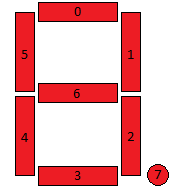
IMPORTANT NOTE: The seven segment displays have a built-in inverter that requires the user to invert the bits in the byte before converting to hexadecimal.
- For example, to program the seven segment displays to display the letter “F”, the portions of the seven segment display that would light up would be 0, 4, 5, and 6. This would make the byte
0b01110001. Remember, the bits must be inverted before converting to hexadecimal. This makes the byte0b10001110, which in hexadecimal is0x8E. Thus, the code for “F” is0x8E.
Code Example
To use the Seven Segment Displays, you must store a value into the memory address of 0xf0a00000. This value is broken into 4 bytes: 1 for each seven segment display.
Each byte section is further broken down into bits, where one bit corresponds for one of the seven(plus decimal point) segments. This breakdown can be seen here:
We can write these segments as binary, where 0 is the least significant bit of a btye and 7 is the most significant bit.
0b11111111
  76543210
Using this format, and adding 3 more bytes to the front(because the Seven Segment Displays panel has 4 actual displays), we can display a wide range of characters on the Seven Segment Displays, although we mostly use it for hexadecimal numbers. Using the Seven Segment Displays often requires the use of a bit of “translating” code to map a decimal value to a seven segment value.
Example:
.org 0x10000000

main:
    li $t0 , 0xf0a00000 # load the memory address for the switches into $t0

    li $t1 , 0xf9a4808e
    # this hex number can be broken into fourths
    #   0xf9 - for the first(left, most significant) digit
    #   this is 0b11111001 in binary
    #   0xa4 - for the second digit
    #   0b10100100
    #   0x80 - for the third digit
    #   0b10000000
    #   0x8e - for the fourth(last, right, least significant digit)
    #   0b10001110
    sw $t1 , 0($t0) # this stores the value into the memory address of the seven segment display
Note: clipboard access is not available on all platforms, results may vary.
Beacause the Seven Segment Displays has an internal inverter(in the actual PLP board), we use 1’s to denote a disabled segment and 0’s to denote enabled segents. That means, this above example would display ‘128f’ on the seven segments.
Additional tutorial: PLP Basic I/O Tutorial
Interrupt Controller
| Register | Description |
|---|---|
0xf0700000 |
Mask |
0xf0700004 |
Status |
Mask Register:
| bit | Description |
|---|---|
| 31-4 | Reserved |
| 3 | Button Interrupt |
| 2 | UART Interrupt |
| 1 | Timer Interrupt |
| 0 | Global Interrupt Enable |
Status Register:
| bit | Interrupt Reason |
|---|---|
| 31-4 | Reserved (Always 0) |
| 3 | Button Interrupt |
| 2 | UART Interrupt |
| 1 | Timer Interrupt |
| 0 | Always 1 |
The interrupt controller marshals the interrupt behavior of the PLP system.
The user uses the two registers in the interrupt controller, mask and status, along with the interrupt registers, $iv and $ir, to control all interrupt behavior. Along with this we have $i0 and $i1 as temporary registers which can be used inside your interrupt service routine.
Before enabling interrupts, the user must supply a pointer to the interrupt vector in register $iv.
main:
  li $iv, isr # put a pointer to our isr in $iv

isr: ...
When an interrupt occurs, the interrupt controller sets the corresponding bit in the status register. Before returning from an interrupt the user must clear any status bits that are resolved or unwanted.
The user enables interrupts by setting any desired interrupts in the mask register, as well as setting the global interrupt enable (GIE) bit. When an interrupt occurs, the GIE bit is automatically cleared and must be set on interrupt exit.
IMPORTANT NOTE: When returning from an interrupt, set the Global Interrupt Enable (GIE) bit in the delay slot of the returning jump instruction. This is necessary to prevent any interrupts from occurring while still in the interrupt vector.
When an interrupt occurs, the return address is stored in $ir.
A typical interrupt vector:
isr:
	li $i0, 0xf0700000
	lw $i1, 4($i0)     # read the status register

	#check status bits and handle any pending interrupts
	#clear any handled interrupts in $i1

	sw $i1, 4($i0)     # clear any handled interrupts in the status register
	lw $i1, 0($i0)     # get the mask register
	ori $i1, $i1, 1    # set GIE

	jr $ir
	sw $i1, 0($i0)     # store the mask register in the delay slot to guarantee proper exit
Timer
The timer module is a single 32-bit counter that increments by one every clock cycle. It can be written to at any time. At overflow, the timer will continue counting. The timer module is useful for waiting a specific amount of time with high resolution (20ns on the reference design).
The timer module supports interrupts, and will trigger an interrupt when the timer overflows. The user can configure a specific timed interrupt by presetting the timer value to N cycles before the overflow condition.
GPIO
The GPIO module connects two of the PLP Board’s I/O connectors to the PLP System, enabling 16 GPIO ports.
There are three registers that are used with the GPIO module:
| Address | Description |
|---|---|
0xf0300000 |
Tristate register |
0xf0300004 |
GPIO Block A |
0xf0300008 |
GPIO Block B |
Each block of GPIO ports on the PLP Board has 12 pins: 8 I/O, 2 ground, and 2 Vdd.
The tristate register controls the direction of data on each of the GPIO pins. At startup and on reset, all GPIO are set to be inputs (the tristate register is zeroed). This protects circuits that are driving any pins on the GPIO ports. The user can set GPIO to be outputs by enabling the tristate pins for those outputs. The tristate bits map to GPIO pins in the following table.
| Tristate Register Bit | GPIO Pin |
|---|---|
| 0 | A0 |
| 1 | A1 |
| 2 | A2 |
| 3 | A3 |
| 4 | A4 |
| 5 | A5 |
| 6 | A6 |
| 7 | A7 |
| 8 | B0 |
| 9 | B1 |
| 10 | B2 |
| 11 | B3 |
| 12 | B4 |
| 13 | B5 |
| 14 | B6 |
| 15 | B7 |
The GPIO registers use the bottom 8 bits of the data word. The other bits are always read 0.
The figure above shows the pin mappings to the below table.
| Pin | Mapping/Bit Position |
|---|---|
| 1 | 0 |
| 2 | 1 |
| 3 | 2 |
| 4 | 3 |
| 5 | GND |
| 6 | Vdd |
| 7 | 4 |
| 8 | 5 |
| 9 | 6 |
| 10 | 7 |
| 11 | GND |
| 12 | Vdd |
VGA
The VGA module controls a 640x480 display with an 8-bit color depth.
An 8-bit color depth provides 3 red bits, 3 green bits, and 2 blue bits per pixel. The blue channel only has two bits because of a bit-depth limitation as well as the human eye’s poor sensitivity to blue intensity.
The VGA module has two registers:
| Address | Description |
|---|---|
0xf0400000 |
Control |
0xf0400004 |
Frame Buffer Pointer |
The control register uses only the least significant bit, which enables or disables the VGA controller output. When the control register is 0, the VGA module is disabled. When the control register is 0x1, the VGA module is enabled.
Enabling the VGA module has significant impact on memory performance. The VGA module uses RAM as VGA memory, and has a higher priority to the RAM bus than the CPU. During a draw cycle, the CPU will not be able to access the SRAM for a short period of time.
The frame buffer pointer is a pointer to the pixel data to draw in memory. For example, if your pixel data begins at 0x100f0000, you would set the frame buffer pointer to that location. The frame buffer must be 307,200 bytes long. The pixel data is arranged as starting from the upper left hand corner of the screen (0,0), and drawing to the right, one row at a time (like reading a book). That is, the zeroth pixel in the pixel data is the upper left hand corner. The upper right hand corner is the 639th pixel, and the left most pixel of the second row is the 640th pixel.
A pixel can be indexed by its row and column address (with 0,0 being the upper left hand corner) with : address = base_address + (640*row) + column.
The chart below displays the order of the color bits in the byte.
| Bit | Color |
|---|---|
| 7 | red[2] |
| 6 | red[1] |
| 5 | red[0] |
| 4 | green[2] |
| 3 | green[1] |
| 2 | green[0] |
| 1 | blue[1] |
| 0 | blue[0] |
- For example, to create a purely red pixel, the code would be
0b11100000in binary, or0xE0in hexadecimal.
PLPID
The PLPID module contains two registers that describe the board identity and frequency. Writing to either register has no effect.
0xf0500000 - PLPID (0xdeadbeef for this version)
0xf0500004 - Board frequency (50MHz, 0x2faf080, for the reference design)
The CPUID module is useful for dynamically calculating wait time in a busy-wait loop. For example, if you wanted to wait .5 seconds, you could read the board frequency, shift right by 1 bit, and call the libplp_wait function.
Performance Counters
| Address | Description |
|---|---|
0xf0800000 |
Interrupts |
0xf0800004 |
I-cache Misses |
0xf0800008 |
I-cache Accesses |
0xf080000c |
D-cache Misses |
0xf0800010 |
D-cache Accesses |
0xf0800014 |
UART Bytes Received |
0xf0800018 |
UART Bytes Sent |
The performance counter module stores a number of registers that keep count of various events, as shown above. Performance counters are read-only and reset only during board reset.
Hardware Configuration and Bootloader
The PLP Board comes with the fload bootloader programmed to the board’s ROM, which starts at power-on and board reset.
The bootloader currently supports three functions:
- Loading data from the UART
- Memory test
- Memory test with VGA module enabled
These three functions are initiated by setting the appropriate switch after power-up. When all switches are unset, the LEDs will scroll indefinitely. When one of the above functions is enabled, only LED 0 will be illuminated.
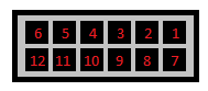
| Switch | Function |
|---|---|
| 0 | UART Boot / Programming Mode |
| 1 | Memory Test |
| 2 | Memory Test with VGA Module Enabled |
The board can be reset at any time by pressing button 0 or BTNL (depending on model) on the PLP Board . This causes all modules and the CPU to reset, setting the PC to 0. This will restart the bootloader.
Loading the Hardware Configuration and Bootloader
If the PLP Board does not have this programmed to the board’s ROM, you must program it before the PLP Board will accept programming from PLPTool or the command line.
To program the PLP Board with the correct hardware configuration and bootloader, you must first download and install the Adept Software required to program the PLP Board.
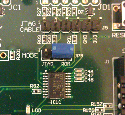
Before running Adept, you must first make sure that your PLP Board has the correct jumper position so that you are programming the ROM of the PLP Board. To do this, make sure the jumper labeled “MODE” is set to ROM. The picture below displays how it should look.
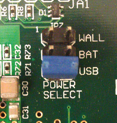
After ensuring the jumper is in the right position, connect the PLP Board to your computer with a micro-USB cable and power on the PLP Board. If the board does not power on once connected and the power switch is in the on position, check to make sure the POWER SELECT jumper is in the USB position. The image below shows how that the jumper should be positioned to receive power from the micro-USB cable.
Next, run the Adept software. Adept will bring a window that looks like the one below.
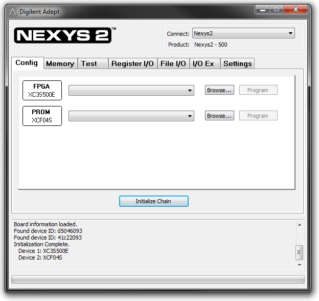
If it does not display the proper board in the “Connect:” dialog box in the upper right-hand corner of the window, then the board has not been connected properly. Make sure that the board is connected and powered on before running Adept.
Next, click Browse… on the line with the box labeled PROM. Navigate to your the directory where PLP is located. The bootloader is located in /hw/.
The file you select will depend on the board you have:
- If you have a Nexys 2 (500k), select the file named
nexys2_500k.bit - If you have a Nexys 2 (1200k), select the file named
nexys2_1200k.bit - If you have a Nexys 3, select the file named
nexys3.bit
Once you’ve selected the correct bootloader file, click the Program button on the same line as PROM. This will load the bootloader onto the PLP Board.
If there are no error messages, the dialog box at the bottom of the Adept window will display Programming Successful. Once the programming is complete, turn the PLP Board off, close Adept, and turn the board back on. Your PLP Board now has the proper hardware configuration and fload bootloader loaded into the ROM and you are ready to program the board using PLP.
Programming the PLP Board
In order to program the PLP Board, the PLP Board must be powered on and connected to the computer via a serial connection. It must also have the correct hardware configuration and bootloader (fload) on the board, as well as be in programming mode. If your PLP Board is not correctly programmed, refer to this section which details how to program the PLP Board with the proper hardware configuration and fload bootloader. To enter programming mode, switch 0 (indicated by SW0 above the switch) must be up/on.
After this is all completed, press the Program PLP Board button. This will bring up the window below.
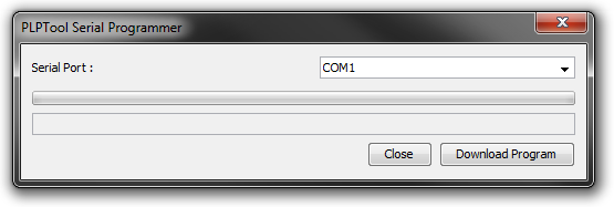
This window allows you to select which port your PLP Board is connected to. There are four preloaded options (COM1, COM2, COM3, and COM4) that can be selected via the drop down menu. If the port you are using isn’t listed, you can enter in the port by clicking in the text box and typing the port’s name.
Once you have selected the correct port, click Download Program, and the program will be loaded onto the PLP Board. If there are any errors, they will be displayed in the Output Pane of PLPTool.